
Features
- Dual-side-cooled PQFN 8x8 package for enhanced thermal performance
- Insulated gate with high threshold voltage and high gate margin
- Built-in freewheeling diode for low reverse conduction voltage drops during dead time
- Negligible reverse recovery charge
- Low gate charge (Qg) and output charge (Qoss)
- High drain-to-source voltage slew-rate (dv/dt) immunity
- Soft- and hard-switching capability
- Transient overvoltage capability
- Increased efficiency in hard- and soft-switched circuits
- Supports higher power density designs
- Compatible with commonly used gate drivers
- Pin-to-pin compatible with E-mode GaN devices with higher threshold voltage for improved noise immunity
- JEDEC qualified
- RoHS-compliant and halogen-free package
Description
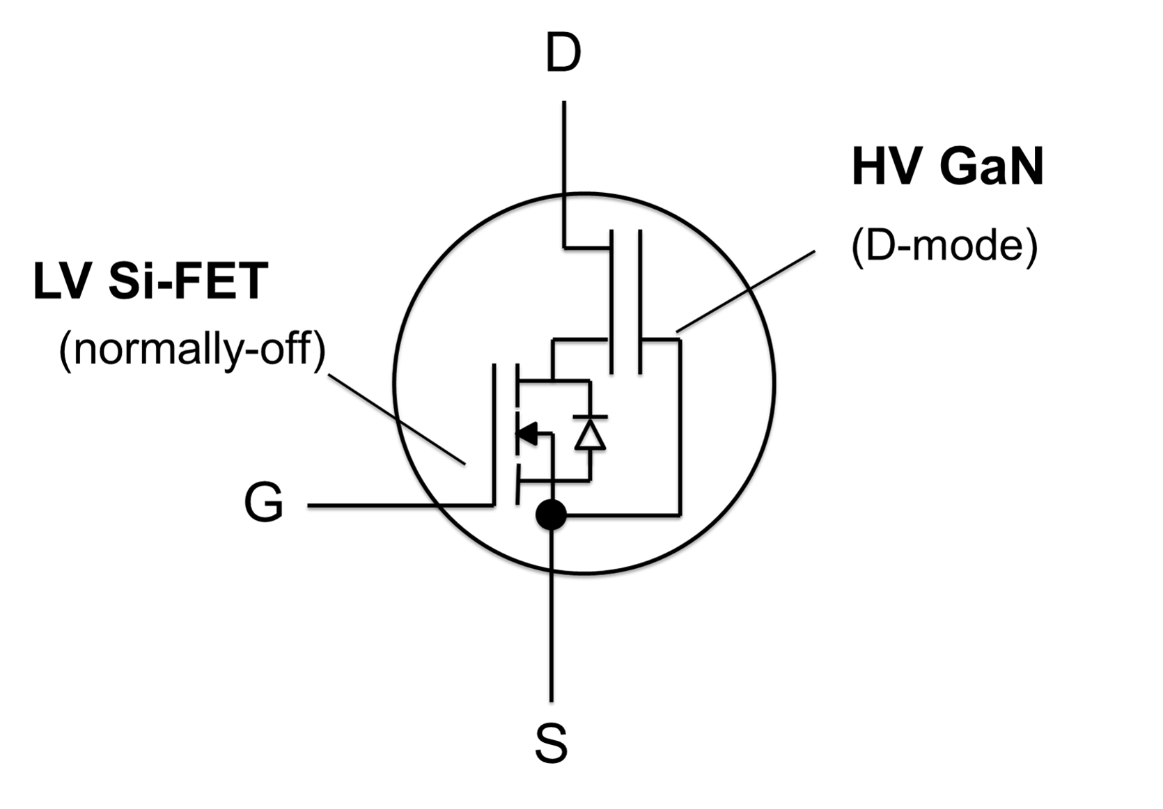
The TP65H020G4PLSGBD is a 650V, 20mΩ gallium nitride (GaN) FET built on Renesas' Gen IV Plus platform. This normally-off switch combines a high-voltage depletion-mode GaN high-electron-mobility transistor (HEMT) for fast switching and high reliability with a low-voltage silicon metal-oxide-semiconductor field-effect transistor (MOSFET) for compatibility with standard gate drivers.
Available in a thin PQFN 8x8 package with dual-side cooling, the TP65H020G4PLSGBD delivers enhanced thermal performance and supports high system-level power density. Its low gate charge, low output charge, negligible reverse recovery charge, and soft- and hard-switching capabilities help improve power-conversion efficiency while reducing system size, weight, and cost.
Parameters
| Attributes | Value |
|---|---|
| Blocking Capability | Uni-Directional Switch |
| Qualification Level | Standard |
| Vds min (V) | 650 |
| V(TR)DSS max (V) | 900 |
| RDSON (Typ) (mΩ) | 20 |
| RDSON (max) (mΩ) | 25 |
| Vth typ (V) | 4 |
| Id max @ 25°C (A) | 92 |
| Qg typ (nC) | 19.6 |
| Qoss (nC) | 221 |
| Ron * Qoss (FOM) | 221 |
| Ciss (Typical) (pF) | 1439 |
| Coss (Typical) (pF) | 196 |
| Mounting Type | Surface Mount |
| Temp. Range (°C) | -55 to +150°C |
Package Options
| Pkg. Type | Pkg. Dimensions (mm) | Lead Count (#) |
|---|---|---|
| PQN88-IP, DSC | 8x8 | 10 |
Application Block Diagrams
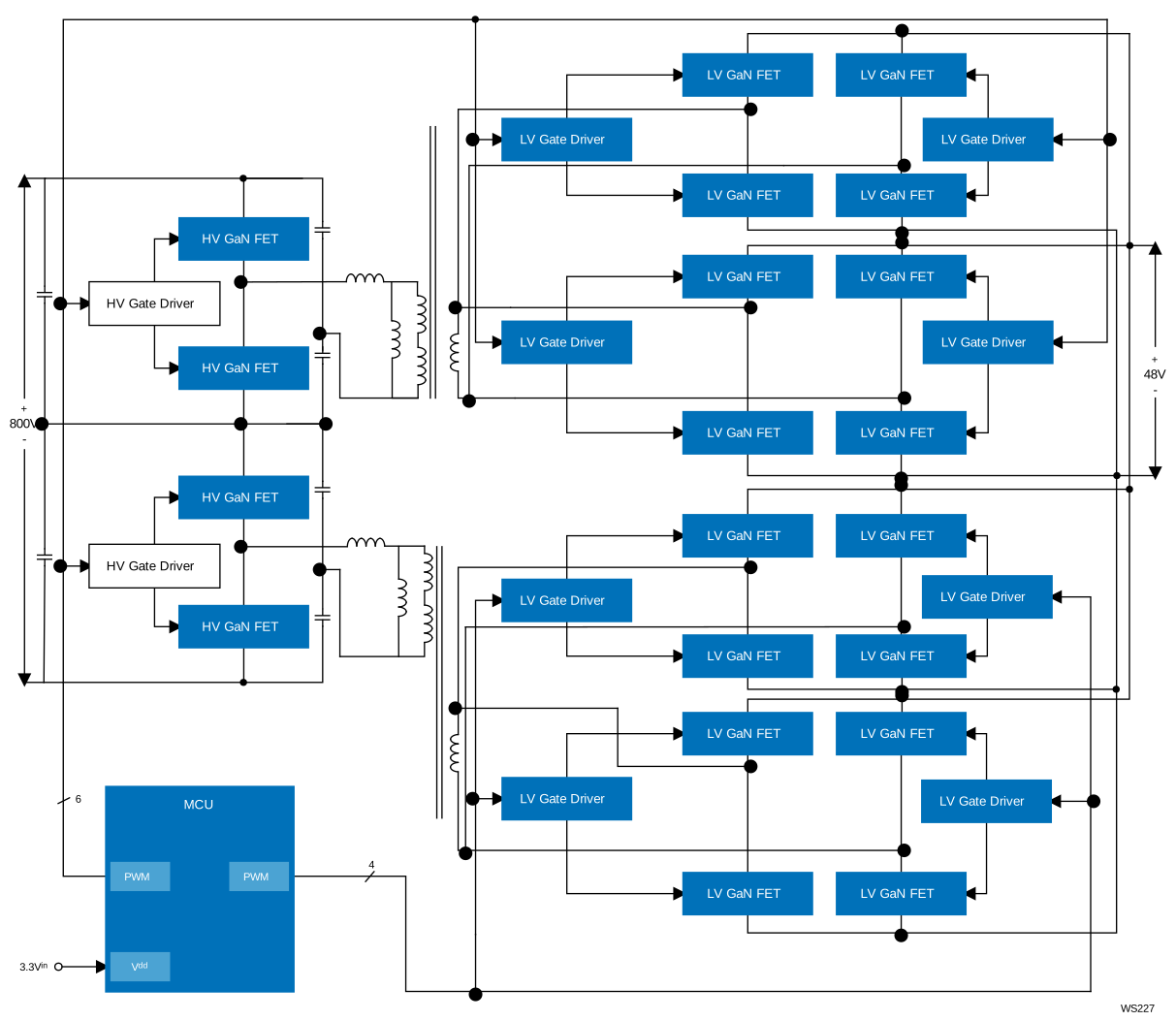 | 800V to 48V DCX System Efficiently converts an 800V DC bus to 48V DC with galvanic isolation for high-density, high-efficiency power delivery. |
Additional Applications
- AI Data Center Power Supplies
- Telecommunications Power Supplies
- Photovoltaic (PV) Inverters
- Uninterruptible Power Supplies (UPS)
- Electric Mobility (e-mobility) Charging
- Battery Energy Storage Systems (BESS)

Support Communities


